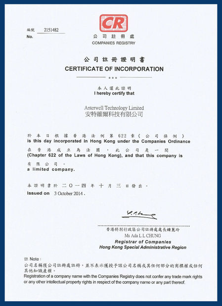
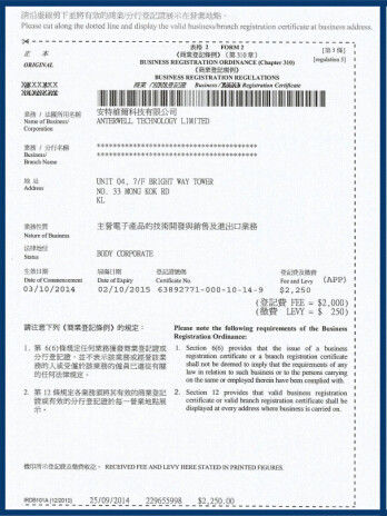
Anterwell Technology Ltd.
Anterwell Technology Ltd.
Large Original stock of IC Electronics Components, Transistors, Diodes etc.
High Quality, Reasonable Price, Fast Delivery.
Anterwell Technology Ltd.
Large Original stock of IC Electronics Components, Transistors, Diodes etc.
High Quality, Reasonable Price, Fast Delivery.
Product Details:
Payment & Shipping Terms:
|
| Storage Temperature: | −65˚C To +150˚C | Lead Temperature (Soldering, 5 Sec.): | 260˚C |
|---|---|---|---|
| ESD Rating: | 2 KV | Input Supply Voltage: | −0.3V To +7.5V |
| Shutdown Input Voltage: | −0.3V To +7.5V | Output Voltage: | −0.3V To +6.0V |
| High Light: | electronics ic chip,integrated circuit ic |
||
Stock Offer (Hot Sell)
| Part no. | Quantity | Brand | D/C | Package |
| MCR100-8 | 9700 | ON | 15+ | TO-92 |
| GT8Q101 | 9778 | TOSHIBA | 16+ | TO-3P |
| LM321MF | 9778 | NS | 16+ | SOT23-5 |
| 2SC1890 | 9800 | HITACHI | 14+ | TO-92 |
| SN74LS74AN | 9800 | TI | 14+ | DIP14 |
| STRW6252 | 9800 | SANKEN | 14+ | TO-220F-6 |
| MC14584BDR2G | 9811 | ON | 16+ | SOP-14 |
| ADM483EARZ | 9855 | AD | 16+ | SOP |
| TLP2631 | 9871 | TOSHIBA | 13+ | DIP8 |
| 74HCT244D | 9878 | PHI | 15+ | SOP |
| LM386N-1 | 9880 | NS | 16+ | DIP8 |
| MOC3041 | 9888 | FAIRCHILD | 16+ | DIP-6 |
| KA1M0565RYDTU | 9955 | FSC | 14+ | TO-220 |
| NE556 | 9970 | ST | 14+ | DIP-14 |
| AO4468 | 9971 | AOS | 14+ | SOP-8 |
| TLP185 | 9985 | TOSHIBA | 16+ | SOP-4 |
| FDN5618P | 9997 | FAIRCHILD | 16+ | SOT23 |
| BC548C | 9999 | ST | 13+ | TO-92 |
| CPC1035N | 9999 | CLARE | 15+ | SOP4 |
| PIC12F629-I/P | 9999 | MICROCHIP | 16+ | DIP-8 |
| TLP291-4 | 9999 | TOSHIBA | 16+ | SOP16 |
| AOD452 | 10000 | AOS | 14+ | TO-252 |
| CS1024 | 10000 | ZX | 14+ | TO-92S |
| FAN102MY | 10000 | FSC | 14+ | SOP-8 |
| HCPL-354-000E | 10000 | AVAGO | 16+ | SOP-4 |
| LM358P | 10000 | TI | 16+ | DIP-8 |
| MOC3022 | 10000 | MOT | 13+ | DIP-6 |
| MOC3063 | 10000 | FSC | 15+ | DIP-6 |
| 74HC157D NXP | 10008 | NXP | 16+ | SOP16 |
| MIC2172YM | 10008 | MIC | 16+ | SOP8 |
LP3872/LP3875
1.5A Fast Ultra Low Dropout Linear Regulators
General Description
The LP3872/LP3875 series of fast ultra low-dropout linear regulators operate from a +2.5V to +7.0V input supply. Wide range of preset output voltage options are available. These ultra low dropout linear regulators respond very quickly to step changes in load, which makes them suitable for low voltage microprocessor applications.
The LP3872/LP3875 are developed on a CMOS process which allows low quiescent current operation independent of output load current. This CMOS process also allows the LP3872/LP3875 to operate under extremely low dropout conditions.
Dropout Voltage: Ultra low dropout voltage; typically 38mV at 150mA load current and 380mV at 1.5A load current.
Ground Pin Current: Typically 6mA at 1.5A load current
Shutdown Mode: Typically 10nA quiescent current when the shutdown pin is pulled low.
Error Flag: Error flag goes low when the output voltage drops 10% below nominal value.
SENSE: Sense pin improves regulation at remote loads
Precision Output Voltage: Multiple output voltage options are available ranging from 1.8V to 5.0V with a guaranteed accuracy of ±1.5% at room temperature, and ±3.0% over all conditions (varying line, load, and temperature).
Features
Applications
Absolute Maximum Ratings (Note 1)
If Military/Aerospace specified devices are required, please contact the National Semiconductor Sales Office/ Distributors for availability and specifications.
Storage Temperature Range −65˚C to +150˚C
Lead Temperature (Soldering, 5 sec.) 260˚C
ESD Rating (Note 3) 2 kV
Power Dissipation (Note 2) Internally Limited
Input Supply Voltage (Survival) −0.3V to +7.5V
Shutdown Input Voltage (Survival) −0.3V to +7.5V
Output Voltage (Survival), (Note 4), (Note 5) −0.3V to +6.0V
IOUT (Survival) Short Circuit Protected
Maximum Voltage for ERROR Pin VIN
Maximum Voltage for SENSE Pin VOUT
Operating Ratings
Input Supply Voltage (Note 6) 2.5V to 7.0V
Shutdown Input Voltage −0.3V to 7.0V
Maximum Operating Current (DC) 1.5A
Junction Temperature −40˚C to +125˚C
Note 1: Absolute maximum ratings indicate limits beyond which damage to the device may occur. Operating ratings indicate conditions for which the device is intended to be functional, but does not guarantee specific performance limits. For guaranteed specifications and test conditions, see Electrical Characteristics. The guaranteed specifications apply only for the test conditions listed. Some performance characteristics may degrade when the device is not operated under the listed test conditions.
Note 2: At elevated temperatures, devices must be derated based on package thermal resistance. The devices in TO220 package must be derated at θjA = 50˚C/W (with 0.5in2, 1oz. copper area), junction-to-ambient (with no heat sink). The devices in the TO263 surface-mount package must be derated at θjA = 60˚C/W (with 0.5in2, 1oz. copper area), junction-to-ambient. The SOT-223 package must be derated at θjA = 90˚C/W (with 0.5in2, 1oz. copper area), junction-to-ambient.
Note 3: The human body model is a 100pF capacitor discharged through a 1.5kΩ resistor into each pin.
Note 4: If used in a dual-supply system where the regulator load is returned to a negative supply, the output must be diode-clamped to ground.
Note 5: The output PMOS structure contains a diode between the VIN and VOUT terminals. This diode is normally reverse biased. This diode will get forward biased if the voltage at the output terminal is forced to be higher than the voltage at the input terminal. This diode can typically withstand 200mA of DC current and 1Amp of peak current.
Note 6: The minimum operating value for VIN is equal to either [VOUT(NOM) + VDROPOUT] or 2.5V, whichever is greater.
Typical Application Circuits
![]()
![]()
Connection Diagrams
![]()
Block Diagrams
![]()
High Power Rectifier Diode 1N4756A , Silicon Planar Zener Diodes
Bridge Type Rectifier Diode 1N4007 50 to 1000 Volts 1.0 Ampere
1N4742A Silicon Planar Zener Diodes for Stabilized Power Supply
Power Programmable IC Chips XC6SLX100-3FGG484C Spartan-6 Family Overview
128K Bytes Sound IC Chip Programming ATMEGA128-16AU 8 Bit Microcontroller
EMC Programmable IC Chips Compliant Slew Rate Limited EI , Timer IC Chip
SMD Power Mosfet Module L7812CV TO-220 Power Trans Electronic Compoents
2SD1594 3 Pin Transistor NEC NPN Power Transistor Switching High Speed
2N5459 Power Mosfet Transistor N-Channel To-92 Original Stock FSC
